Join Us
Prospective students and early-career researchers
Nano Photonics Research Group
Find your path in materials-to-chip optoelectronics.
We welcome motivated students and early-career researchers who want to grow through real experiments, careful device physics, academic writing, and collaboration across materials, photodetectors, imaging systems, and chip-level integration.
Opportunities
A focused research environment with a clear student path
Work Alongside The Team
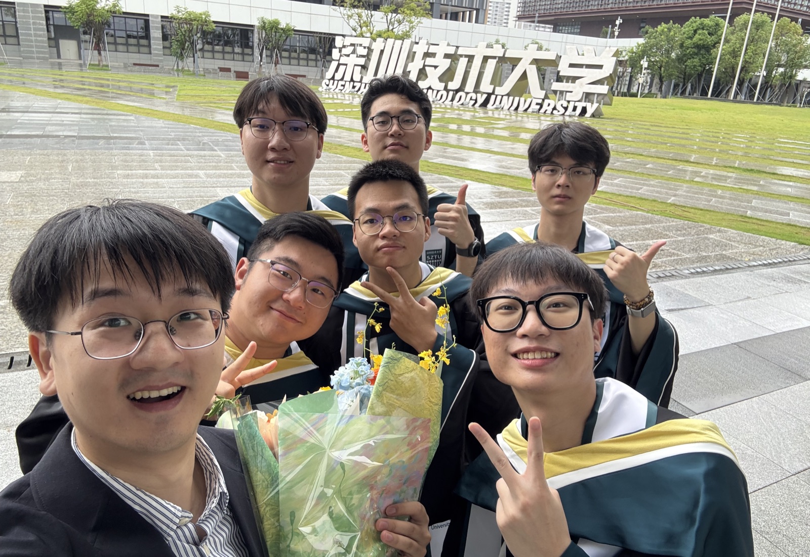
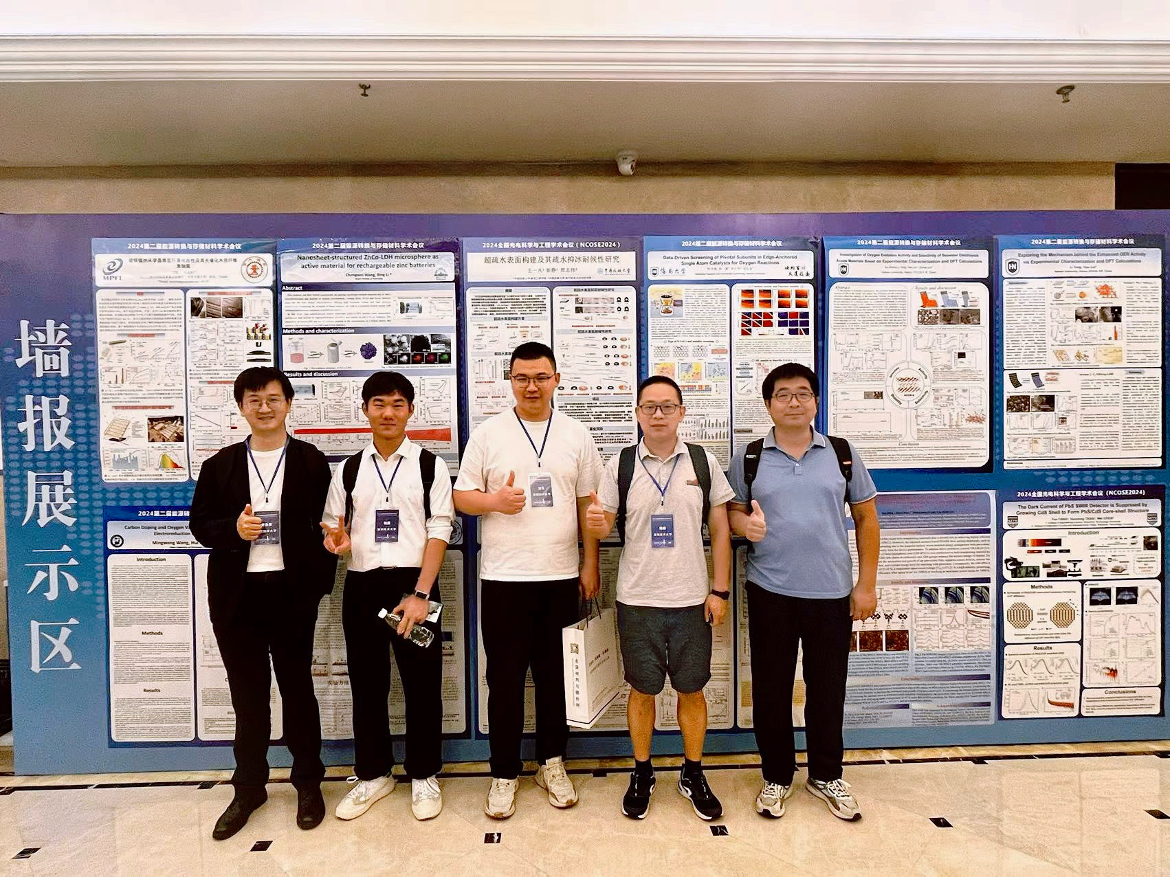
New students learn by taking part in the whole research process: reading papers, preparing materials and devices, measuring results, discussing data in group meetings, and turning careful experiments into clear research stories. The group also values the everyday parts of academic growth, from conference posters and manuscript revisions to graduation milestones.
Research Directions
Quantum-dot and perovskite optoelectronic devices, SWIR photodetectors, imaging arrays, thin-film processing, interface engineering, transient spectroscopy, and CMOS-compatible integration.
Training Environment
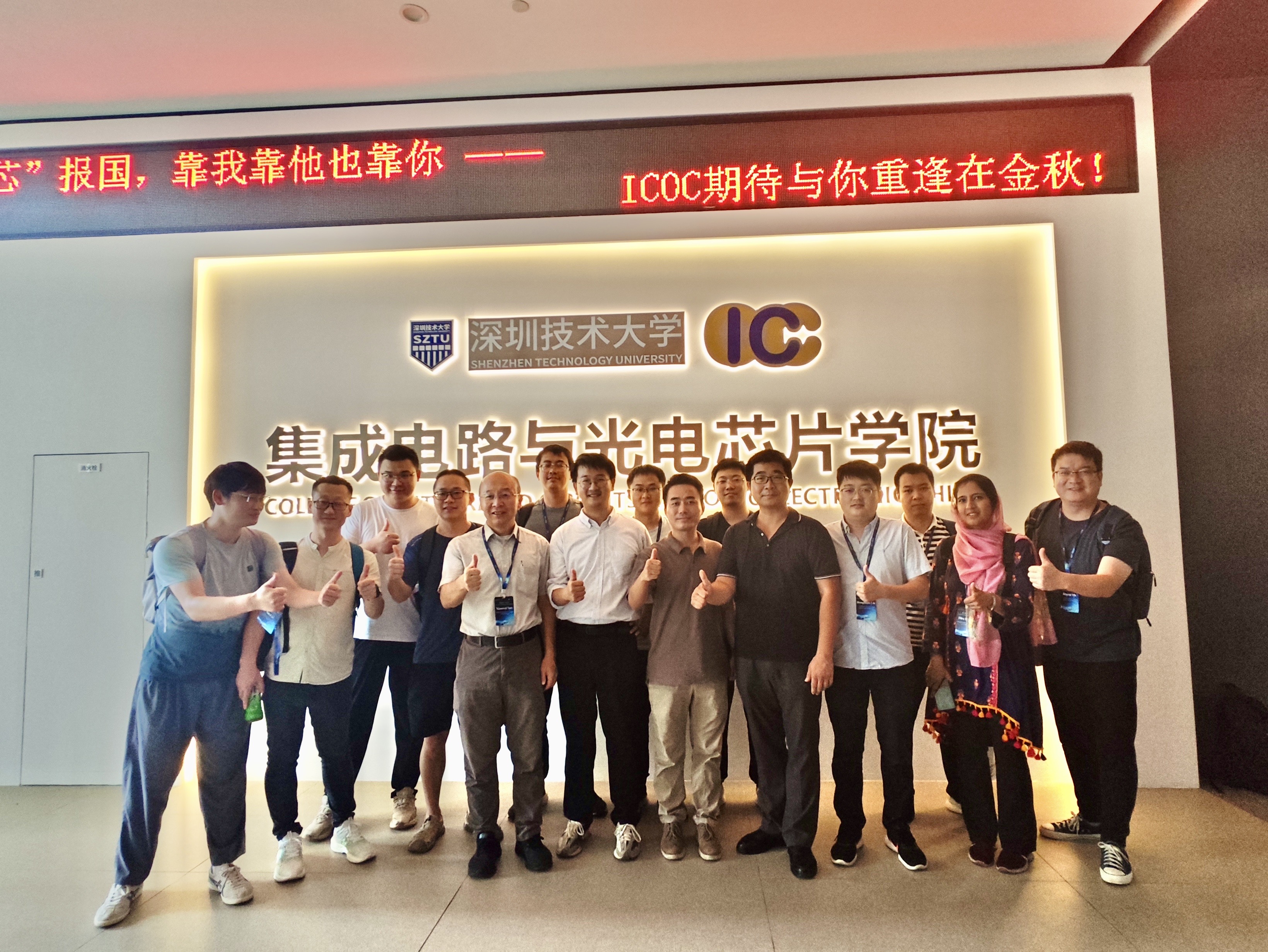
Hands-on device research, mentoring across materials and chips, access to fabrication and characterization workflows, publication coaching, group discussions, and opportunities to present research at academic meetings.
Who Should Apply
Students from microelectronics, optoelectronics, materials science, physics, chemistry, computer science, automation, or related fields. Evidence of curiosity, responsibility, and sustained technical work matters more than already knowing our exact topic.
How To Apply
Make the first email specific enough to evaluate
Send These Materials
- CV or resume
- Transcript
- Representative projects, papers, code, or design work if available
- A short note on your research interests, preferred start time, and the group direction you want to discuss
Suggested Subject
[2026 Master/PhD Application - Name - University - Major]
Contact
What We Look For
You do not need to arrive with complete experience in quantum dots or chip fabrication. What matters most is evidence that you can keep moving a concrete problem forward: reading papers, keeping records, reproducing experiments, analyzing data, and explaining results clearly.
What New Students Do
New students usually begin with literature reading, basic fabrication, device measurement, and data organization, then move toward independent projects linked to papers, conference presentations, graduation work, or future graduate study.